Wafer Dicing is a critical process in the semiconductor industry, which involves the separation of individual dies from a wafer. The process is essential in the production of electronic devices such as microprocessors, memory chips, and sensors. Wafer dicing is typically performed after the wafer has undergone various fabrication processes, such as photolithography, etching, and deposition, to create multiple layers of integrated circuits on a single substrate.
The primary goal of wafer dicing is to separate the individual dies with high precision and accuracy without damaging them. This process involves several steps, including alignment, cutting, and separation. The most used wafer dicing technique is mechanical dicing, which uses a blade to cut the wafer into individual dies. Other techniques include laser dicing and plasma dicing, which use high-energy beams to cut the wafer.
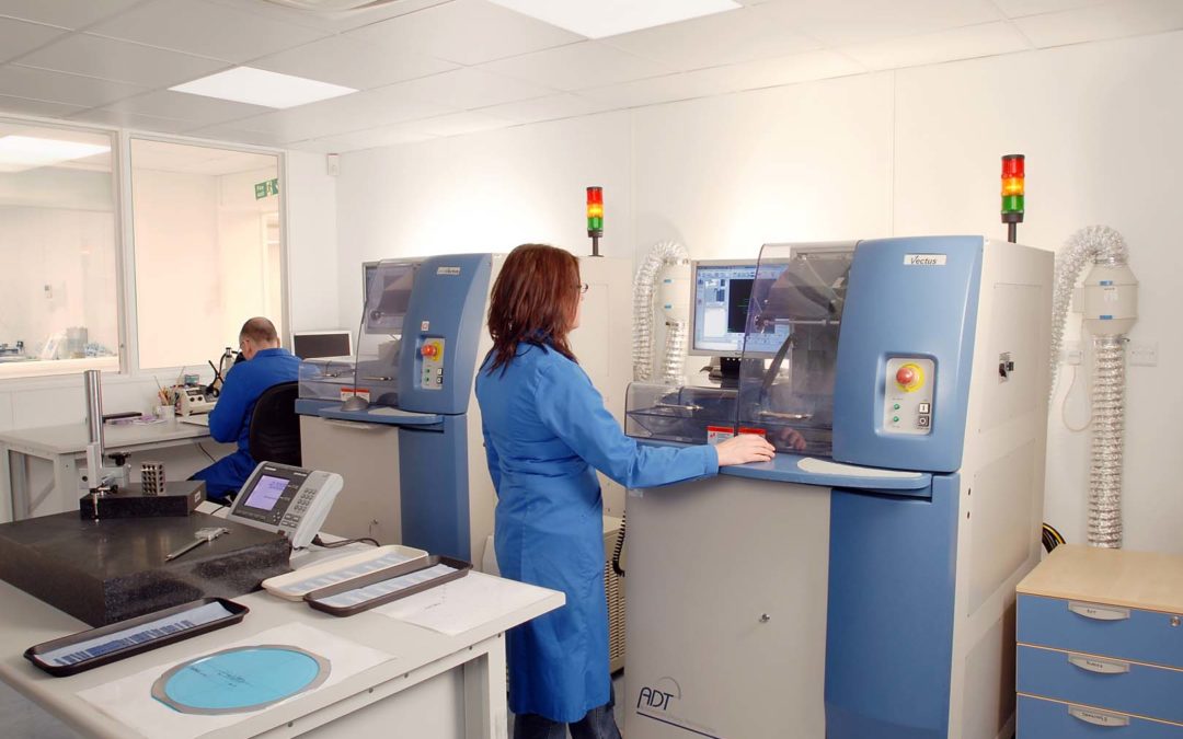
Mechanical Dicing
Mechanical dicing involves mounting the wafer onto a tape or film, which provides support during the cutting process. The wafer is then aligned with a diamond-tipped blade, which cuts through the wafer along the pre-determined scribe lines. The blade is typically cooled with a water-based coolant to prevent overheating and minimize the risk of chipping or cracking the wafer. After the cutting process is complete, the individual dies are separated from the remaining wafer material using a pick-and-place tool or a vacuum wand.
Laser Dicing
Laser dicing, on the other hand, uses a high-energy laser beam to cut through the wafer. The laser beam is focused on the wafer surface, creating a localized heat zone that causes the material to fracture along the scribe lines. Laser dicing is often used for cutting brittle materials such as silicon carbide, sapphire, and gallium nitride, which are difficult to cut with mechanical blades.
Plasma Dicing
Plasma dicing is a relatively new technique that uses a low-pressure plasma to etch the wafer along the scribe lines. The plasma contains reactive species that react with the wafer material, causing it to fracture along the scribe lines. Plasma dicing is often used for cutting thin and fragile wafers, which are susceptible to damage during mechanical cutting.
Wafer Dicing for silicon, sapphire and other materials can be up to 200mm in diameter which requires high precision and accuracy to avoid damaging the dies and maximize the yield of the fabrication process. Mechanical dicing is the most commonly used technique, but laser dicing and plasma dicing are also gaining popularity due to their ability to cut brittle and fragile materials.
For all your Wafer dicing services you require please contact us here
