Thin Film Deposition
Metalisation and passivation
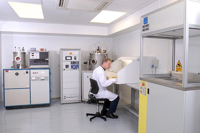
ICT has been undertaking thin film deposition services, such as metalisation of ceramics and plastics, at its Shepperton facility, for over 20 years.
Thin film deposition is used for a number of component products, including deposition of ceramic components for inkjet printers. It is also used for metalisation of plastic components, such as those used in sensors. ICT is actively involved in assisting clients with sensor design and prototyping and welcomes enquiries from anyone involved in new product design or product development projects.
ICT’s deposition equipment includes:
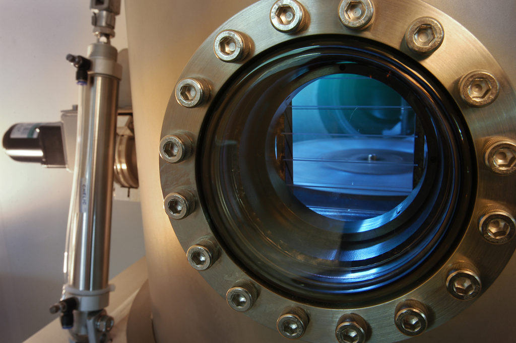
- Triple source DC magnetron 24”sputter system
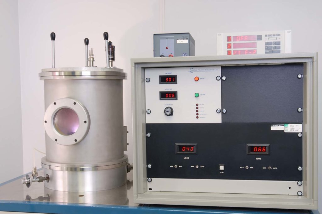
- Single source RF magnetron 12” sputter system (SiO2)
- OPTIMAL UCS 40MF Automatic Cleaning System
ICT uses a smaller single source RF magnetron chamber (12”) for laying down a passivation layer, typically two microns of silicon dioxide (SiO2).


Quality Assured
ICT undertakes rigorous pull testing to record and monitor the quality of the metalisation process to ensure compliance with stringent standards, on a batch by batch basis.
Where metalisation is used for wire bonding purposes, a pull test using wire bonding is used. ICT also has a Dage pull tester.
All components go through an OPTIMAL automatic cleaning system prior to deposition.
For more information on ICT’s quality assurance and quality control procedures, go to ICT’s quality assurance.
Want more information or a quote?
If you have a sputtering or thin film deposition job that you would like to discuss with an ICT engineer,
please call us now on +44 (0)1932 509911.


