Latest Blogs
Why Precision Lapping Is Critical for Photonics Substrates
Photonics technologies are at the forefront of innovation across industries including telecommunications, medical diagnostics, aerospace, and advanced sensing. At the heart of these technologies lie photonic substrates - materials such as silicon, indium phosphide...
Precision Engineering in Photonics Device Fabrication
Why microscopic tolerances and post fabrication process control determine whether a photonics device succeeds in the real world. Photonics devices play a critical role in modern technology, enabling advancements in telecommunications, medical diagnostics, sensing, and...
What is an Advanced Semiconductor?
Advanced semiconductors are the foundation of today’s most demanding technologies, enabling faster processing, lower power consumption, smaller devices and greater functional integration. From artificial intelligence and 5G communications to medical diagnostics and...
What Are Semiconductors and Why Do They Matter?
What Are Semiconductors? Semiconductors are specialised materials whose electrical conductivity falls between that of conductors - like copper, and insulators - like rubber. This unique intermediate behaviour makes them the fundamental building blocks of modern...
What is a MEMS Sensor?
What is a MEMS Sensor? Micro-Electro-Mechanical Systems (MEMS) sensors are miniature devices that combine mechanical elements, sensors, actuators, and electronics on a common silicon substrate. Manufactured using techniques derived from semiconductor wafer processing,...
Chip-on-Board Assembly Explained: A Guide to High-Density Electronic Packaging
Chip-on-Board Assembly Explained: A Guide to High-Density Electronic Packaging As electronic devices continue to shrink while performance expectations rise, manufacturers are increasingly turning to advanced packaging techniques to achieve higher functionality in...
What is Wire Bonding?
Wire bonding remains one of the most established and reliable interconnect technologies used in microelectronics manufacturing. Despite the emergence of alternative packaging techniques, wire bonding continues to play a vital role across semiconductor, medical,...
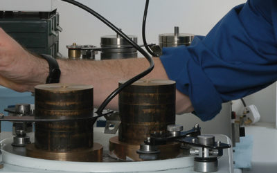
Mastering Precision: The Art and Science of Precision Lapping
In the realm of precision manufacturing, where tolerances are measured in microns and the slightest imperfection can spell disaster, precision lapping stands as a pinnacle of accuracy and finesse. From aerospace components to medical devices, the applications of...
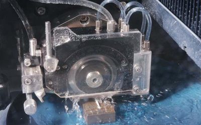
What is Micromachining?
Micromachining is the procedure of creating very small and extremely intricate structures with high precision. This technology has transformed the manufacturing of microelectromechanical systems (MEMS) and is used in a range of devices, including smartphones, medical...
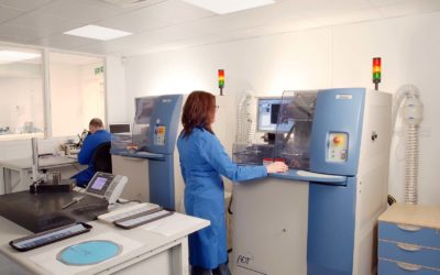
What is Wafer Dicing?
Wafer Dicing is a critical process in the semiconductor industry, which involves the separation of individual dies from a wafer. The process is essential in the production of electronic devices such as microprocessors, memory chips, and sensors. Wafer dicing is...


